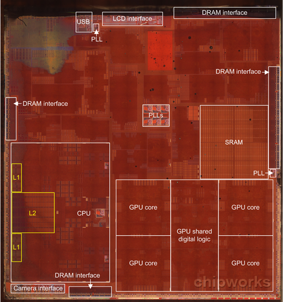
Following their initial analysis of the iPhone 5s’s innards, silicon experts at Chipworks have now taken a closer look at the handset’s 64-bit A7 processor to reveal a number of interesting tidbits in their initial low-level chip analysis. Based on transistor-level images of the Apple-designed, Samsung-built package, Chipworks was able to determine that the A7 consists of a dual-core processing core and quad-core graphics, tentatively identified as the four cluster version of Imagination Technologies’s PowerVR Series 6, the G6430.
Apple, along with Intel, is of course an investor with a ten percent stake in Imagination Technologies, the UK-based fabless semiconductor maker. Chipworks also focused on a portion of the A7 chip called Secure Enclave where Apple says fingerprint profile is stored securely and walled off from the entire system, except the Touch ID circuitry…
As can be seen on the transistor-level shot top of post, the A7 is a so-called system-on-a-chip, a design that combines pretty much everything a mobile device needs on a single piece of silicon: from CPU/GPU cores to shared logic, memory and other interfaces, RAM, cache, controllers and more.
Although it’s yet to perform a real circuit extraction to confirm the findings, Chipworks preliminarily concluded that the dual-core CPU is Apple’s own design based on the ARMv8 architecture, not the licensed ARM A53/57 design.
The CPU core likely incorporates 256KB of L1 cache and 1MB of L2 cache. They have not determined whether the A7 packs in 1GB of RAM or more. Note that four GPU cores is a step up from the three-core GPU inside the iPhone 5’s A6 processor.
The chip itself is thought to be fabbed on Samsung’s advanced 28-nanometer Hi K metal Gate, which is the same process technology Samsung employs for its own Galaxy S4 Exynos processor.
The dual-core CPU and cache make up ~17 percent of the die area, and the quad-core GPU and shared logic about 22 percent.
As for the chip’s Secure Enclave, Chipworks explains:
Actually, if we compare it with the A6, that may not be such a stupid idea – there is no comparable block that I can see in there.
I wouldn’t have thought that a fingerprint scan would create that much data, but given that multiple scans have to be stored, and in any orientation, maybe that much storage is needed.
One thing we do know is that it’s the biggest fingerprint sensor that we’ve seen so far, coming in at ~39 mm².
Secure Enclave is part of the A7 chip, as depicted on the screenshot below grabbed from Apple’s promo vid.
Chipworks estimates that Secure Enclave is basically a huge block of SRAM with at least 3MB of storage capacity. It’s found right above the GPU cluster.
The A7 also shares a few design similarities with its predecessors, the A5, A6 and A6X, such as the USB, LCD and camera interfaces. Chipworks will be taking apart the Touch ID sensor and posting their observations in another post and I’ll make sure to keep you in the loop.
I’m curious about Apple’s design and engineering approach to AuthenTec-built Touch ID. For the time being, Touch ID is the most advanced, reliable and seamless fingerprint sensor on any device.
Yesterday, I analyzed Samsung’s biometrics efforts to conclude that the Galaxy maker is at least a year away from implementing fingerprint scanning on its smartphones.
“We are not yet developing the technology,” a Samsung official told The Korea Herald.
In its previous analysis of the flagship iPhone 5s, Chipworks has identified a number of design wins. The A7 processor is still being manufactured by Samsung, while the M7 motion coprocessor is basically a rebranded NXP LPC18A1 unit.
The handset’s back-facing iSight camera uses Sony’s Exmor-RS sensor, the front-facing FaceTime shooter is from OmniVision and the accelerometer is made by Bosch.
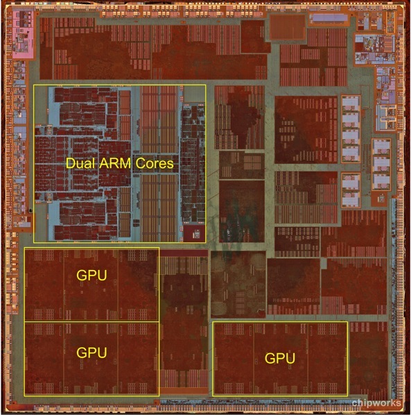
Pictured above, for comparison’s sake: the A6 floorplan.