Apple is thought to become the first customer that will take advantage of Taiwan Semiconductor Manufacturing Company’s (TSMC) InFO chip manufacturing process in building in-house designed A10 chips for 2016 iOS devices, potentially allowing it to trim some fat off the next iPhone model.
Taking a step back to take a look at the bigger picture, we analyze Apple’s chip efforts thus far and make educated guesses as to what advances in terms of silicon design and integration the next iPhone might allow.
We’ll also reflect on how having the foresight to take its chip destiny into its own hands more than five years ago has helped Apple differentiate itself from competition.
What is InFO?
An acronym for Integrated Fan-Out, InFO is a chip process technology that doesn’t require a chip to be fitted on a substrate before being mounted onto a circuit board. InFO is said to help reduce the thickness of a typical mobile chip by 0.2 mm or more.
But what the heck are substrates, you ask…
Also called diffusion layers, substrates define where chip features like the conductors and the connections between the conducting layers are implanted on a logic board.
The engine that drives your iPhone isn’t connected directly to the printed-circuit board due to its small footprint. Instead, it’s fitted on a package substrate which then connects the chip die to the logic board and distributes input-output signals over the entire die.
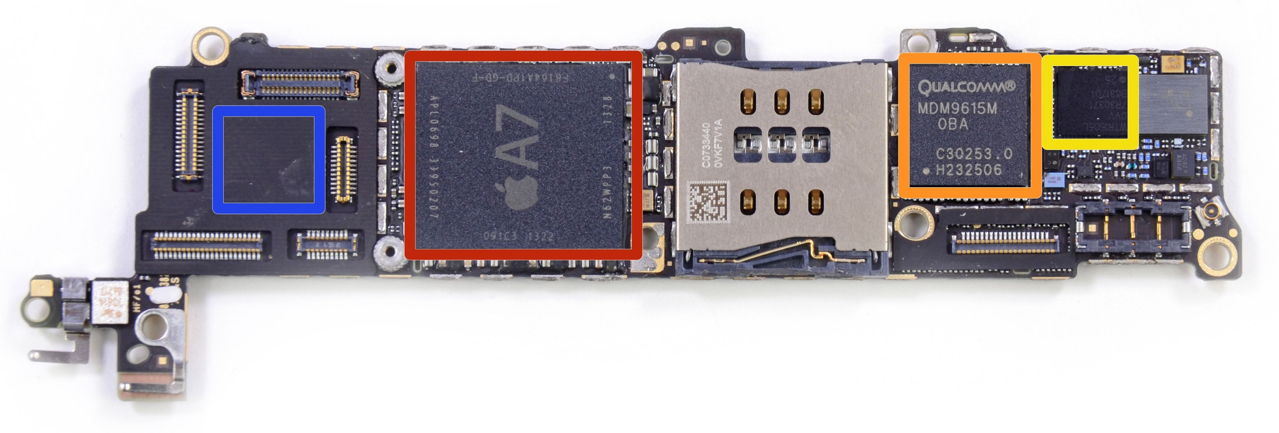
iPhone 5s A7 processor fitted on a substrate connected to the logic board.
But as TSMC is reportedly on the cusp of solving yield issues, its InFO process using a 16-nanometer node should be ready by the time the next iPhone’s A10 processor enters mass production.
Bernstein Research believes that using InFO to mount the A10 directly onto the iPhone’s circuit board will help reduce the overall thickness of the handset.
And because the shorter distance between logic die and printed circuit board also enables faster thermal dissipation, chip speed could increase by 20 percent as a result.
By the way, supply chain sources claimed recently that TSMC will handle all A10 orders exclusively, leaving Samsung entirely out of the picture.
SoC vs. InFO vs. SiP
Speculating further, Apple’s rumored use of TSMC’s InFO process for the next iPhone paves the way for other advancements, such as SiP. An acronym for System-In-Package, this technology essentially packs an entire computer architecture onto a single chip, usually by stacking multiple silicon dies atop each other.
Contrast SiP approach to Apple’s current A9 and A9X mobile chips that combine some, but not all features onto a single die. Specifically, the A9/A9X combine a fully-customized ARM-based dual-core CPU, dubbed ‘Twister,’ 2 GB of LPDDR4 RAM, L1/L2/L3 cache, an image processor, an embedded M9 motion coprocessor and graphics cores onto a single die.
This is known as a system-on-a-chip (SoC) approach.
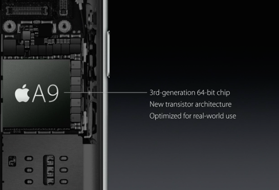
Apple’s ‘A9’ SoC in iPhone 6s has 70% faster CPU and 90% faster graphics. Its predecessor, the A8, has two billion transistors.
As mentioned, the A9 chip is connected to the iPhone 6s’s logic board via a substrate. Removing it would let Apple engineers to mount an iPhone’s SoC and other dies directly onto an even smaller printed circuit board.
This approach of combining multiple dies on a circuit board is known as System-in-Package design, as seen on the Apple Watch’s ‘S1’ chip.
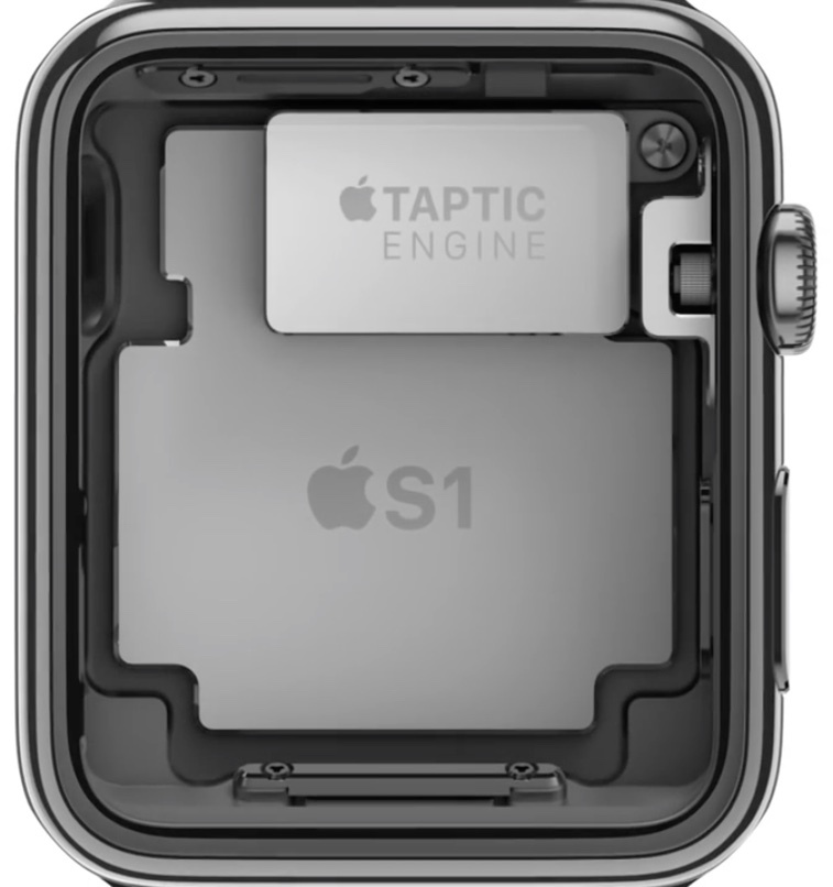
Apple Watch’s resin-encapsulated ‘S1’ uses system-in-package (SiP) design.
iPhone 7: not just thinner, but waterproof?
Should Apple manage to embed wireless chips and sensors—which are currently separate chips—into its own SoC, the next iPhone could have fewer, smaller chips.
And if that package is covered in resin, like with the Apple Watch, Apple should be able to engineer a fully waterproof iPhone that will require less power while running faster.
Apple building own wireless chips, too
Conveniently enough, VentureBeat claims that Intel has put more than 1,000 engineers on a project to adapt its lauded 7360 LTE modem chip for Apple, so it could be embed in the iPhone 7′ A10 SoC.
Apple’s silicon engineering can be traced as far back as 2007, when it started buying semiconductor startups to assemble an internal team which now counts 1,000+ wireless and chip designers.
Deciding to take its chip destiny into its own hands was a tremendously risky move, one that has now paid off in ways more than one.. You can see it in iPhones and iPads consistently outperforming the commodity chips used by its Android competitors, in terms of both speed and performance per watt.
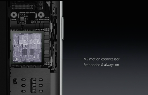
‘M9’ motion coprocessor, previously a separate chip, is now embedded in iPhone 6s’s ‘A9’ system-on-a-chip.
If Apple and its chip manufacturers succeed in embedding an LTE modem and other remaining iPhone chips in the A10, the company will leap even further ahead of competition in terms of custom silicon design.
More food for thought
Looking beyond the iPhone, including the cellular modem would make an Apple SoC a lot smaller, and thereby more likely to fit inside an Apple Watch. A 3G/LTE-equipped Apple Watch would make for a 100 percent standalone wearable device, one truly untethered from your iPhone.
Make no mistake, radio interface chips rival CPUs in complexity—that’s why iPhones and iPads have traditionally used wireless chips from Broadcom and Qualcomm.
But as it’s now surpassed Intel in performance, who’s to say Apple won’t add wireless functionality to its SoCs?
To quote Steve Cheney, Apple designing its own iPhone modems has “physical layer impacts on bandwidth, connectivity, latency and user experience,” all of which are “critical for autonomous vehicles.”
What are your thoughts on Apple’s chip design efforts? And what do you think the future holds in terms of Apple’s chip destiny?
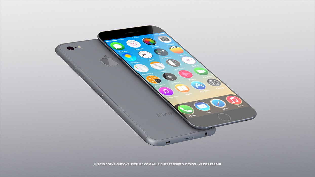
iPhone 7 concept top of post by 3D artist Yasser Farahi.