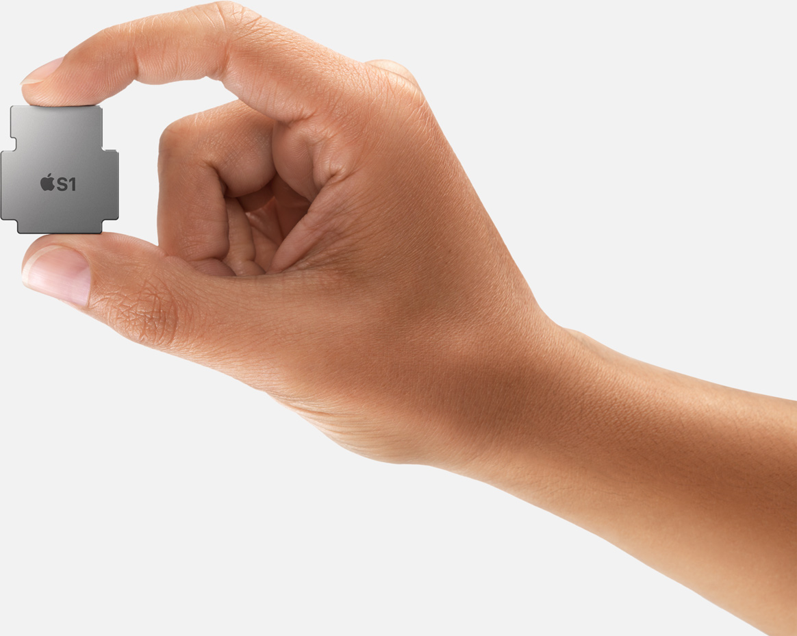
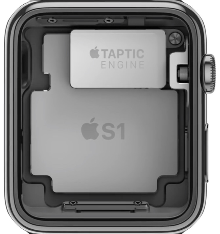
At the heart of the Apple Watch is Apple’s in-house designed ‘S1’ component that literally puts an entire computer architecture onto a single chip — an industry term you’re looking for is system-in-package (SiP) design.
A recent teardown analysis by ABI Research has managed to identify 512MB of RAM, an ARM-based CPU, a Broadcom Wi-Fi module, an accelerometer and gyroscope, along with a few other components, packed inside the S1.
Today, semiconductor experts over at Chipworks have updated their teardown of the S1 package with a few interesting tidbits related to the type of process technology used while revealing some rather unique design solutions making such small yet powerful package possible.
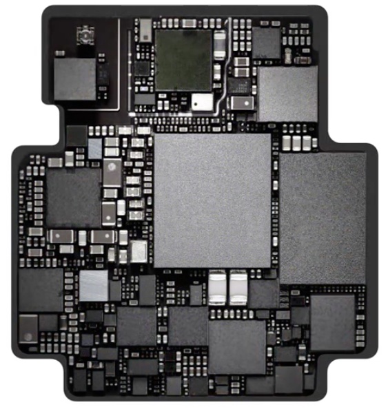
The S1 contains as many as thirty individual components combined in some unique ways and sealed inside the tiny package that measures just 26mm x 28mm.
“It’s quite an accomplishment,” Chipworks noted.
As it turns out, Apple has once again turned to Samsung’s component-making arm to fabricate the application processor (AP) for the Apple Watch. Application processors are usually CPUs capable of running code in a mobile operating system environment.
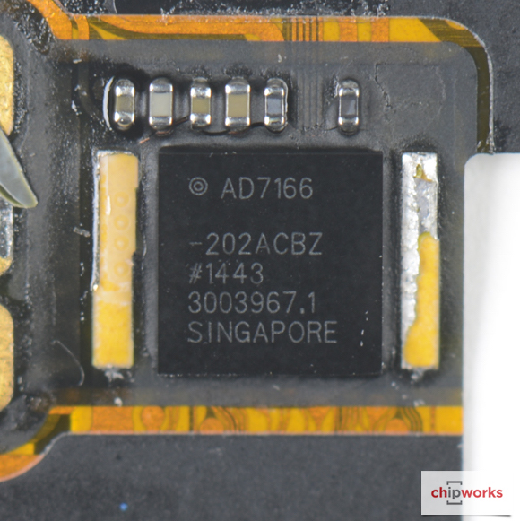
The AP inside the S1 bears the marking ‘APL0778’. It combines the central processing unit (CPU) with an integrated PowerVR SGX543 graphics processing unit (GPU) from Imagination Technologies.
It’s fabbed on Samsung’s low-power 28-nanometer (nm) process technology.
By comparison, Motorola’s Moto 360 smartwatch uses a Texas Instruments OMAP 3630 processor built on an older 45nm process that Apple’s A5 chip inside the iPhone 4s used. The iPhone 6 and iPhone 6 Plus use 20-nanometer application processors marketed under the ‘A8’ moniker.
28nm is also the same process technology used to fabricate Apple’s A7 chip found inside the iPhone 5s and iPad Air. The Qualcomm Snapdragon 801-805 chips were built on the 28nm process up until a few months ago, as were Nvidia’s K1 processors.
Samsung is now moving to a 14-nanometer process and Apple is rumored to use it for an upcoming ‘A9’ chip that should power 2015 iPads and iPhones. That said, it doesn’t take a genius to figure out that the next Apple Watch is likely to contain an even more compact ‘S2’ chip.
If built on a smaller-than-28nm process technology, it would permit faster performance, lower power consumption and a smaller die size, potentially freeing up room for some of the health sensors that reportedly didn’t make it into the current version of the Watch.
Seen below: the sealed S1 package.
Remarkably, the new application processor measures just 5.2mm x 6.2mm.
In a manner similar to earlier versions of Apple’s mobile processors that power older iPhones and iPads, the S1 takes advantage of the package-on-package (PoP) assembly, an integrated circuit packaging method that combines vertically discrete logic and memory packages.
Inside the S1, the package-on-package assembly contains the aforesaid Apple-designed application processor and its dynamic RAM (DRAM) die, installed atop each other with a standard interface to route signals between them. This allows higher component density in such a tiny wearable device.
The same PoP process is used to combine the NXP-supplied NFC circuitry for Apple Pay (controller and radio) with its secure element (Secure Enclave in Apple’s parlance), tasked with storing tokenized payment information and isolating it from other subsystems.
The S1 package is pretty unique in term of manufacturing, too. “The two key words here are system and package,” notes the teardown analysis.
Again, Apple’s suppliers had to cram over thirty remarkable tiny individual pieces of silicon into a 26mm x 28mm package.
All these components are soldered to a common motherboard which is then overmolded with a packaging compound containing silica or alumina spheres suspended in a resin to protect the electronics.
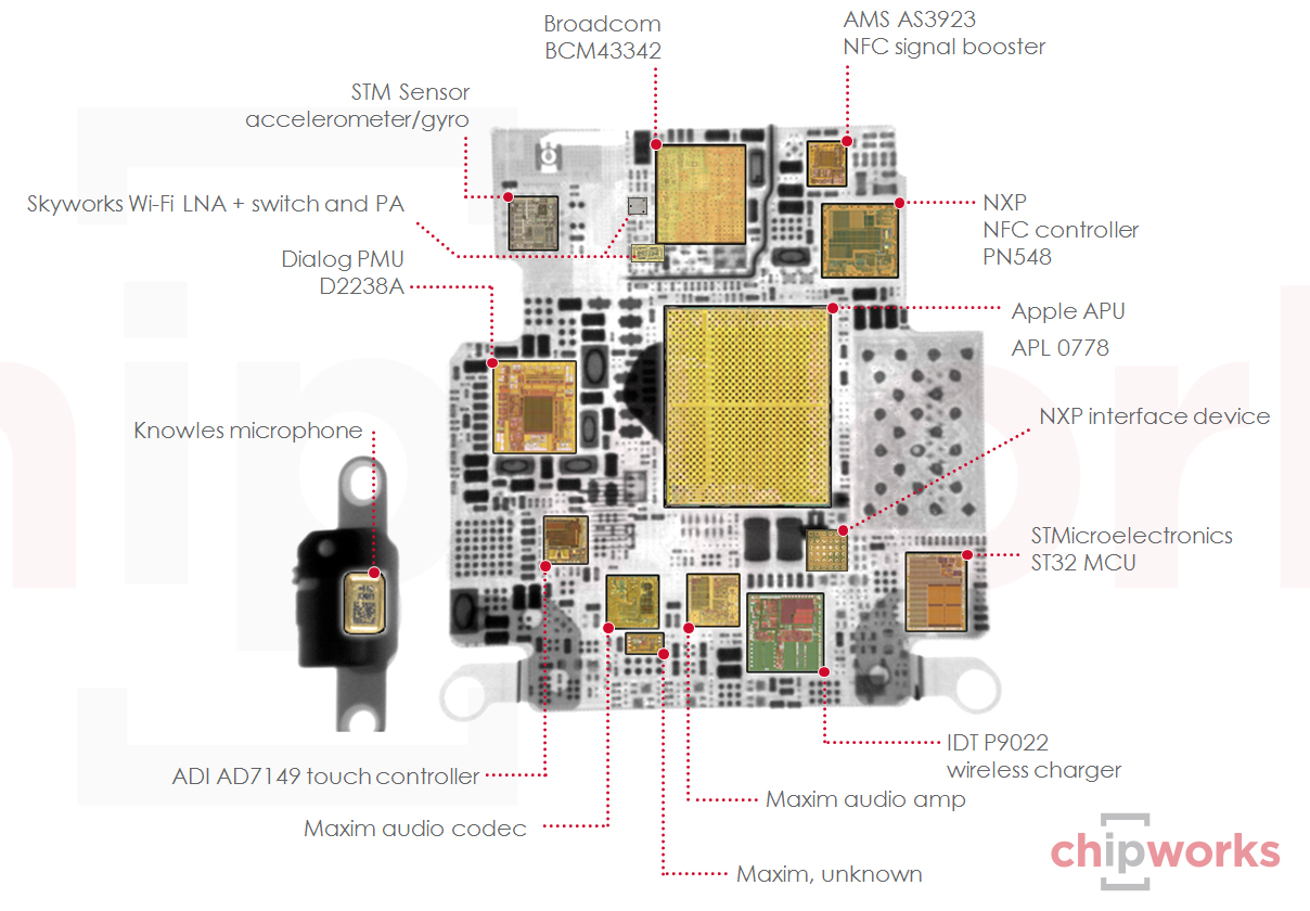
Here’s an overview of the many different component inside the S1 package, as depicted in the promotional Apple Watch video.
“We see this same type of material in conventional IC packaging, but we have never observed this being used over a 26mm x 28mm motherboard,” said Chipworks.
The teardown analysis identifies a few interesting wins in terms of suppliers. For example, the power management integrated circuit socket is provided by Dialog, while the codec and amplifier sockets are supplied by Maxim.
This is different than several iPhone and iPad models, which used to run a Cirrus-branded power management chip. Texas Instruments has six wins in the S1 ranging from battery management to opp amps. The image below clearly shows the Texas Instruments’ OPA2376 Precision oop amp chip inside the S1.
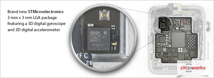
STMicroelectronics got to provide the six-axis sensor for acceleration and roll, pitch and yaw (gyroscope), as well as the ST32 MCU Flash memory micro controller (based on the ARM Cortex‑M processor) and the optical emitter/sensor encoder die located under the shaft of the Watch’s Digital Crown.
Even the aforementioned six-axis sensor is unique in that it marks the first time an Apple product has used an integrated sensor which doesn’t require an external accelerometer. By comparison, both the iPhone 6 and iPhone 6 Plus pack in a six-axis sensor from Invensense and an additional three-axis accelerometer by Bosch.
Interestingly enough, the Watch’s six-axis accelerometer and the second touch controller are not contained within the S1 package.
I’m really impressed by Apple’s work here.
Not only are these engineering achievements commendable given the Watch’s compact design, but most other vendors don’t really bother with expensive semiconductor R&D anymore and instead buy whatever off-the-shelf components are available on the market.
But Apple’s been charting its own silicon future for years now.
Tapping its internal team of more than a thousand silicon engineers, the company actually conceives and designs how these micro components fit together and then produces blueprints for chip foundries like Samsung to fabricate the S1 in volume.
I’m really excited to learn even more about the S1 as Chipworks and other teardown wizards delve deeper into this remarkable piece of silicon, that I don’t have any doubts rivals will have a really hard time replicating this time around.
Source: Chipworks