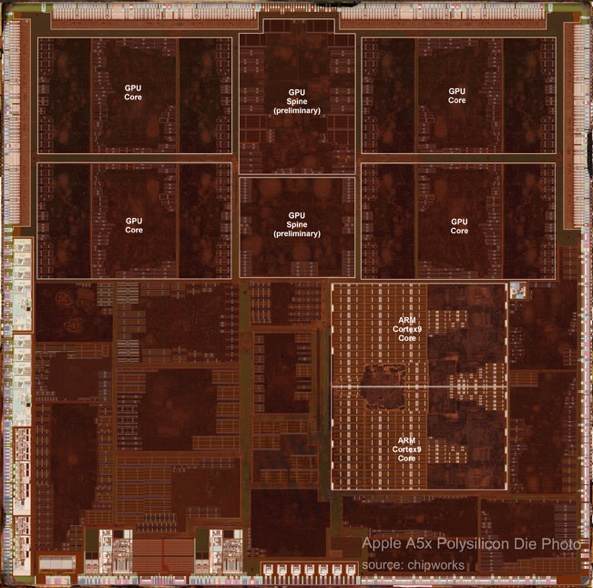
While guys over at iFixIt have done their trademark awesome job peeking under the new iPad’s hood, one aspect of its bowels hasn’t been scrutinized yet: the Apple-designed A5X chip labeled “S5L8945X” and fabbed on Samsung’s 45-nanometer process. Enter silicon analysis firm Chipworks which just released a high-resolution photo depicting so-called “floorplans” of the A5X package.
Their analysis corroborates speculation on the A5X architecture and offers a fascinating insight into the innards of the A5X package. As you can see in the above shot, a large portion of the A5X’s die is dedicated to the four graphic cores, found to be comparable to Nvidia’s Tegra 3 chip in terms of speed.
Apple does not publicly specify the type of GPU/CPU used, but it’s been widely rumored that the A5X packs in Imagination Technologies’ PowerVR SGX543MP4 technology versus a dual core PowerVR SGX543MP2 GPU found inside the A5 chip from iPad 2 (both pieces of silicon run dual-core ARM Cortex-A9 MPCore CPU). Read on for the nitty-gritty details depicted in the polysilicon die photos…
Chipworks confirms that the A5X breaks away from the package-on-package design which stacks memory ball grid array packages atop the discrete logic, with a standard interface to route signals between them. What this means is that the A5X silicon is not packaged together with the RAM.
For the A5X, Apple has also changed packaging, away from what has been package-on-package with the DRAM to putting the DRAM physically on the other side of the board. This type of packaging has been reported to have (theoretical) disadvantages in BoM simplification because it is no longer one module and in performance because of the more routing between the chip and memory. […] We expect that in the future, as Apple moves to newer lower power process technology at 32 nm and below (perhaps employing high-k metal gates) that we’ll see a return to PoP designs.
Interestingly, Chipworks wonders whether the move to a new layout might have created “potential heat issues”. As you know, we’ve found out today by way of thermal imaging and Consumer Reports that the new iPad gets warm when its GPU is put to its limits in graphics-heavy games such as Retina-optimized Infinity Blade II.
As for the size, the A5X package measures 165 mm² – that’s more than three times the size of the A4 package (53.3 mm²). For comparison, Nvidia’s Tegra 3 is 82 mm². Increasing the size of the package in order to squeeze in more components is really a temporary measure until Apple finally moves its chip production to TSMC’s 22-nanometer process, as rumored.
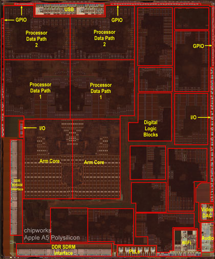
Check out another shot right below depicting a floorplan of the previous-generation A5 package.
Depicted above: The previous-generation A5 package.
Though the A5X system-on-a-chip features power-savvy design, the need to drive four times the pixels coupled with the high-resolution Retina display and 4G networking led Apple to incorporate a lot bigger battery inside the new iPad with 70 percent more capacity than the iPad 2.

